8. Electronics production
Group assignment:
Individual assignment:
Make and test the development board that you designed to interact and communicate with an embedded microcontroller.
Go to:
Group work
In group work we were to characterize the design rules for in-house PCB production process: document feeds, speeds, plunge rate, depth of cut (traces and outline) and tooling. We documented our results to the group work page which is on our Fablab Oulu pages. Check out our results!
Reflection
This week in group work I learned for example:
In our local lecture we were first shown how the milling bit works. You have to take into account the size and shape of the milling bit (and the degree tip angle), copper thickness and depth of cut. For example the 0.1 mm v-bit you use for high detail work. V-bits, or v-carve bits, create a pass shaped like a "v" and are commonly used for detailed engraving.
You can't say a constant value for the depth of cut, and the milling bit used, copper thickness and for example the board being perfectly level or not affects the results. Copper thickness is usually 35 um (0.03500000mm). We used double sided tape for attaching the material. Our test pieces came out nice, but I don't know how precise level you can get with a tape.
These milling bits are very fragile, so you can't drop them down and when changing the tool or adjusting for origin, you have to be careful. The smaller the degree in tip angle, the more fragile the bit is. For example from 30-90 degrees milling bits are commonly used for milling PCBs.
On the other hand, the lower the degree, the more detail you can get (a 60-degree bit will give you more detail than a 90-degree bit).
Our instructor demonstrated us how the degree of the tip angle affects the width of the cut. The wider the angle, the deeper the cuts and more material is removed on the surface. Also because the width of the engraving tool varies based on depth, warped or inaccurately measured boards can result in inaccurate traces.
In our test pieces, we see that the milling bit 0.1 mm does very precise and good work. Only smaller lines than under 0.004 start to disappear. Some of the thinner lines on the bottom of the design started to fall off, but we also had a piece of tape bothering the milling process so I'm not sure if it was also affecting the result. With the 0.2 mm milling bit we see that lines thinner than 0.008 are not working out. Also in the other end, it seems that some of the thicker lines are combined together.
Making the board
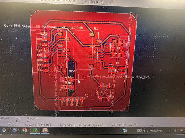
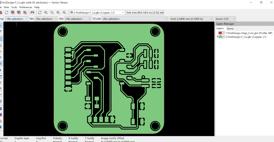
In Electronics design week we designed our board. In KiCad it looked like this:
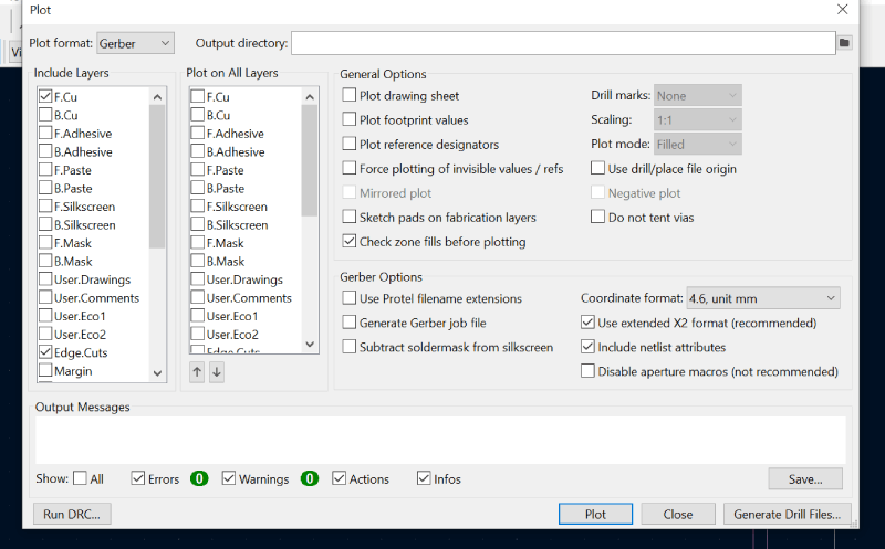
To make the board, I needed to generate Gerber files for my layers. The design was open in PCB editor. I opened File -> Plot. I included F.Cu and Edge cuts -layers. In general option the tab for Check zone fills before plotting was enabled. Then I just pressed plot. The GBR files were saved in to my design project files.
In the main window of KiCad, I opened Tools -> Gerber viewer to see the results.
In Gerber viewer, I chose File -> Open Gerber plot files.
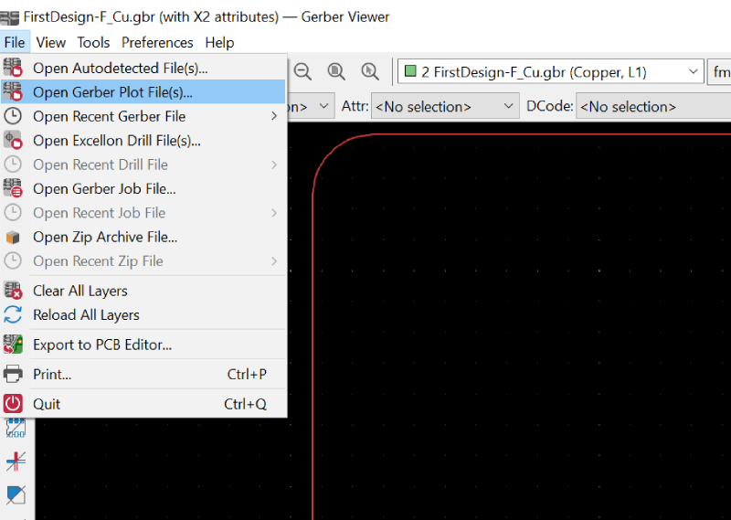
Here you can check the layers. Everything looked good for me.
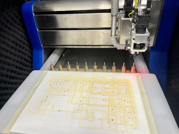
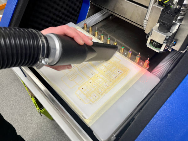
I took my files with me and went to the LPKF machine. Before opening the program I looked that everything was ready. The layer that the material comes on top of, seemed to be alright. Our instructor guided us to anyway do some vacuuming so that absolutely nothing remains under the material because the board needs to be even.
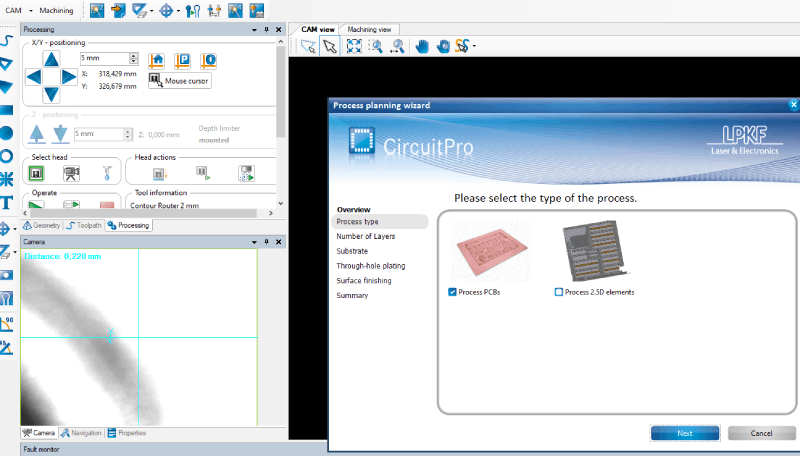
At this point I opened LPKF Circuit Pro program on the computer. I opened up a new project.
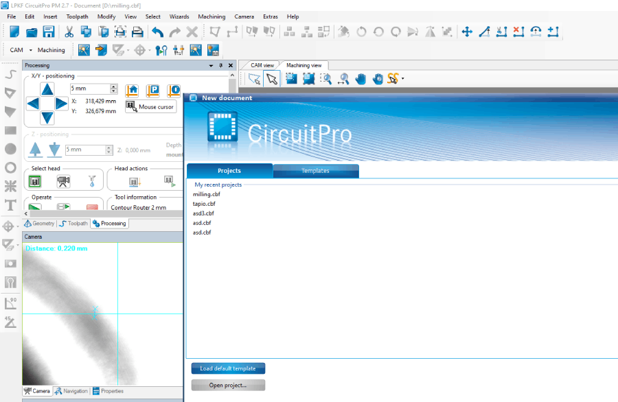
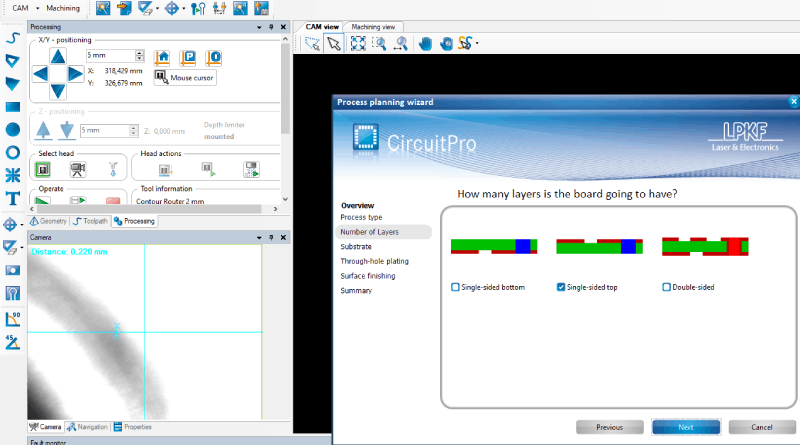
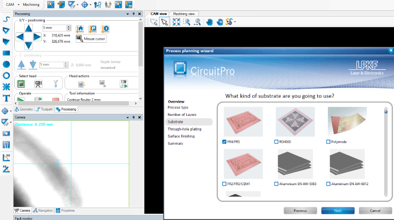
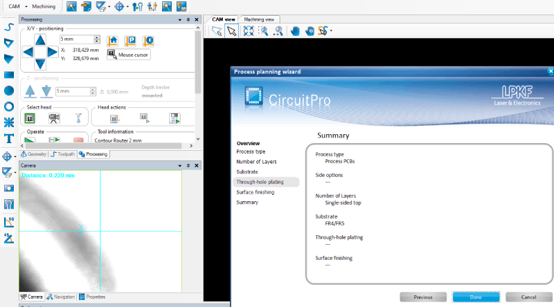
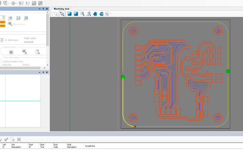
Pretty much everything I needed here was a few buttons on the panel, and I started with the Process planning wizard. Here are the first steps:
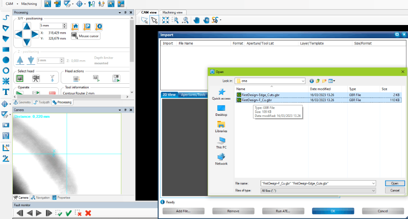
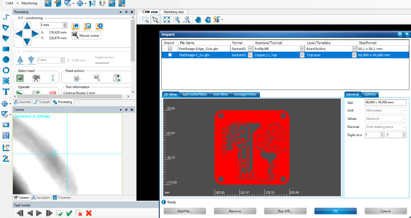
Then I imported my Gerber files.
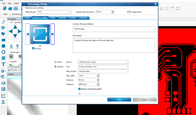
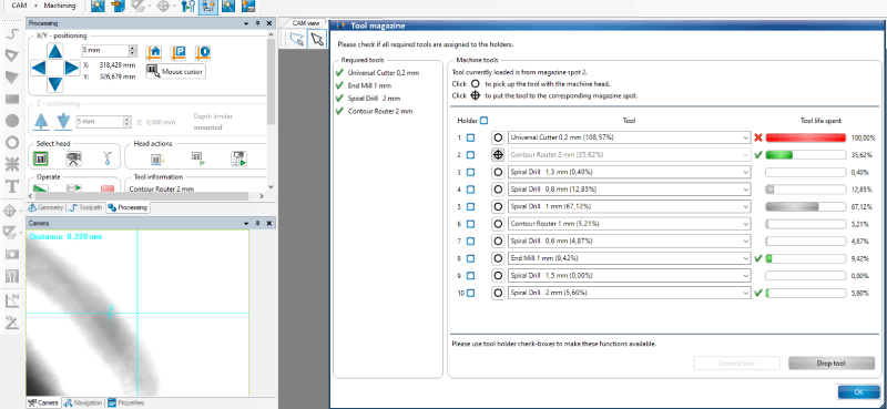
Then I opened the Technology dialog.
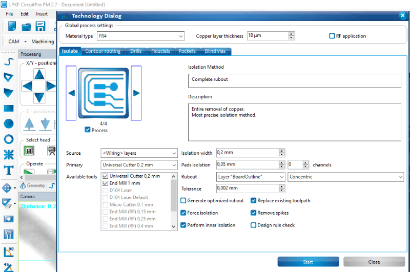
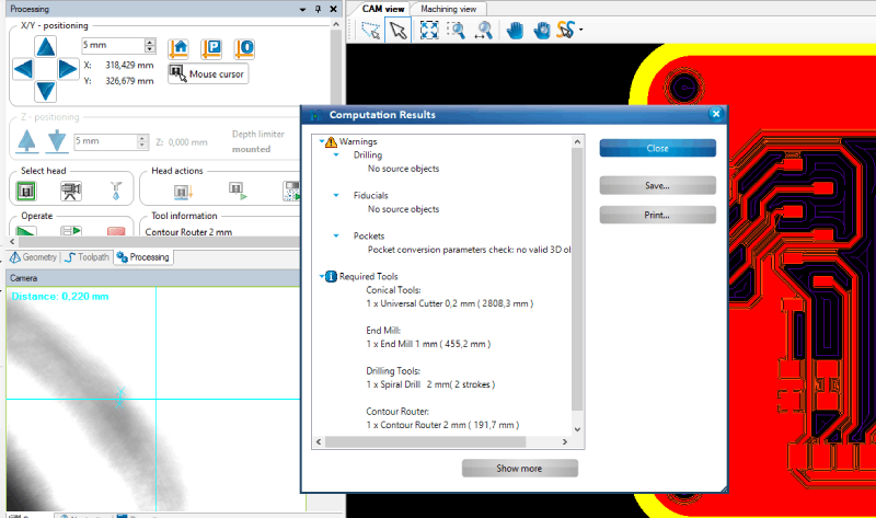
On Tool Magazine the tools needed were shown and also the expectancy of their lifetime. 4 different tools were needed. The universal cutter 0,2 mm needs soon changing, but right now it had still done good work so I went with the old one.
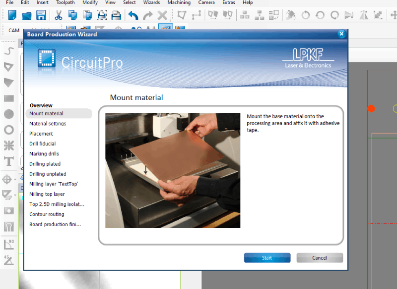
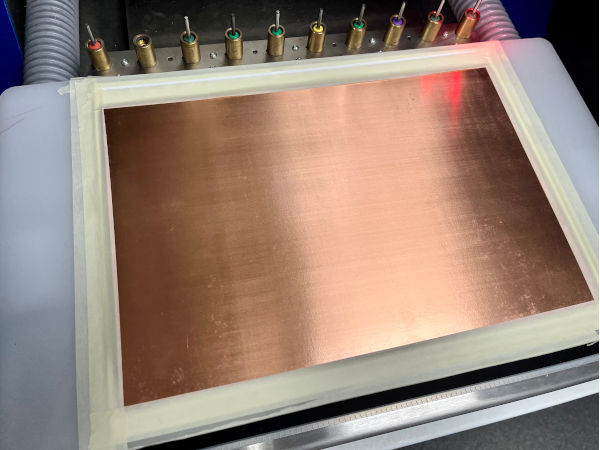
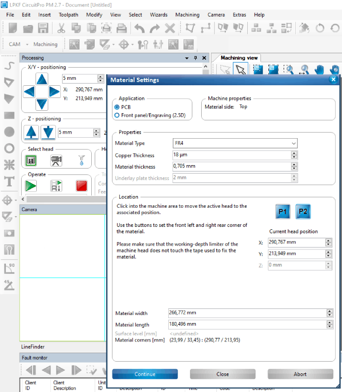
Now the Board production wizard told me I needed to mount my material. So I placed the FR1 on the surface and taped it down on each of it's sides.
In Material settings I now needed to set the coordinates. I clicked in to the board area first choosing a place on down left corner to start. By pressing P1 I set it. Then I clicked on to upper right corner of the area and pressed P2.
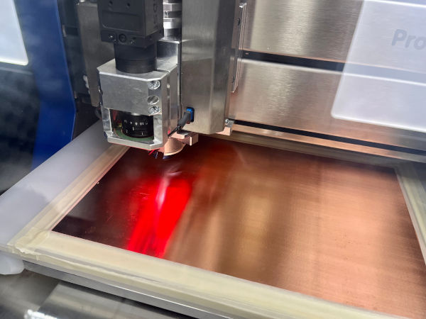
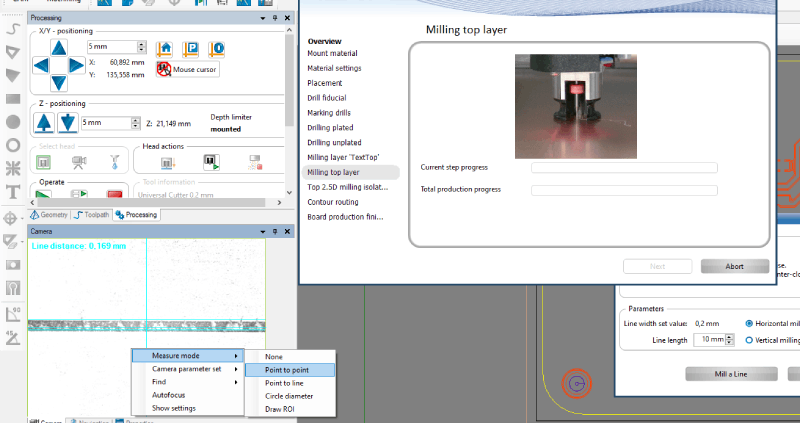
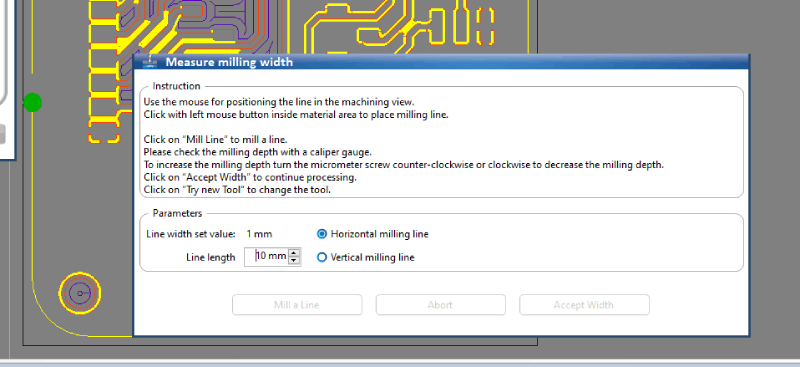
I was set to mill the first layer! The wizard wanted me to calibrate and measure milling width from a line. I clicked to just above my design, and pressed mill a line. The machine went in and milled a 0.2 mm line, and after that went over it with a camera.
On the camera screen I right-clicked to Measure Mode and chose Point-to-point. I measured a distance of 0.207 which was good. I pressed Accept Width.
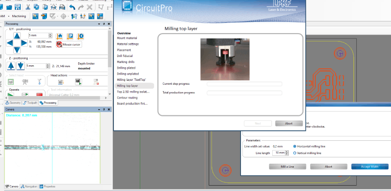
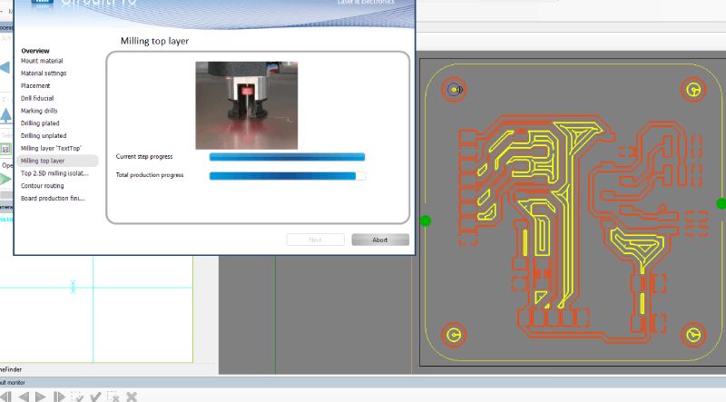
The milling could now start! It was fun to see the process going on the screen also.
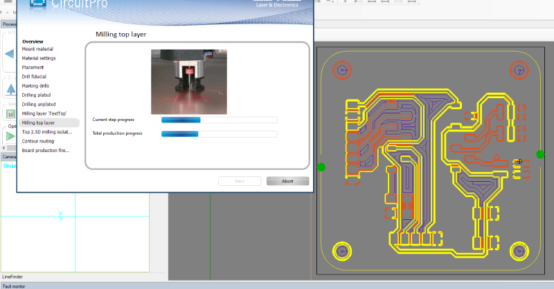
In some point the program wanted to measure milling width again, this time it made a small circle it removed the copper from. As everything looked good, again I pressed Accept width and it went on with the areas that copper needed removing.
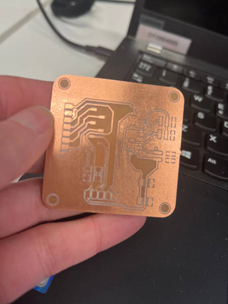
And soon it was done!
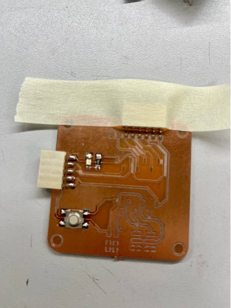
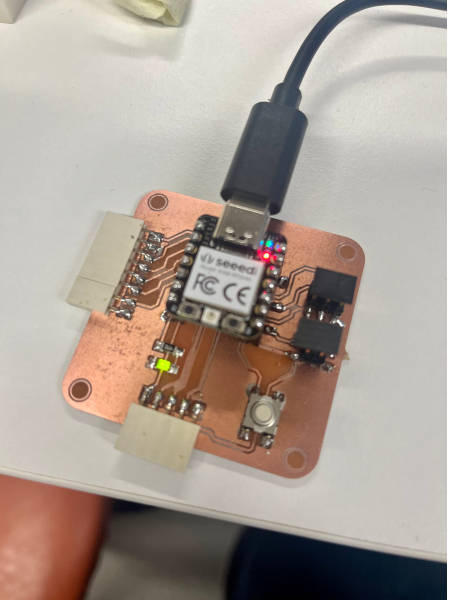
This was the beauty that came out!
Assembly and soldering
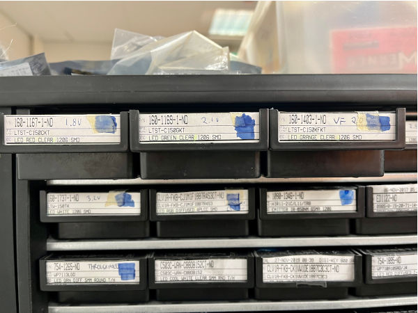
Now that the board was ready, I went on to collect the components needed. We have this tall tower of components on the lab, and a lot of small print on the labels. Fortunately our instructor helped us to find the right parts. For a LED I chose a green one. Here are all the parts:
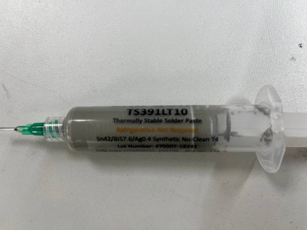
I was going to solder the parts into the PCB, but gladly we also got to try putting them in the oven with some soldering paste. In this way I prepared the LED, resistor and the button.
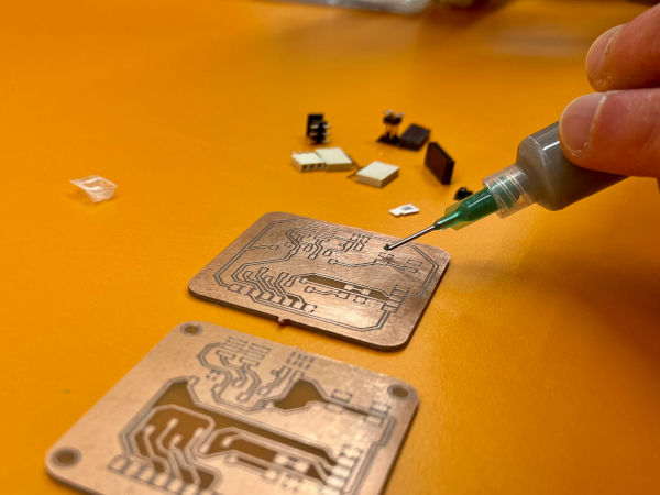
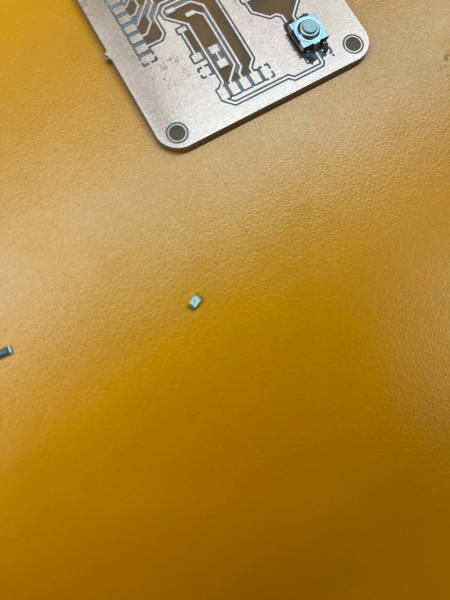
It felt easy to apply the paste. The LED and the resistor were so tiny though, that they did a couple of disappearance trics on me before I got them on.
At this point the UPKF oven was set up with a program by our instructor. The temperature needed to be low enough for these parametres. It started to preheat itself before we put our boards in.
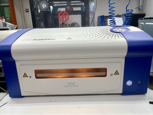
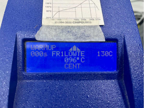
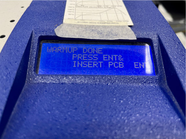
I pressed enter and the door opened. We had two boards going in at the same time, and we placed them somewhere in the middle on the rack.
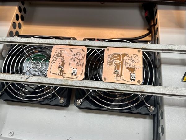
It didn't take long until the oven was signalling it was ready with the work. We took them out and the results looked good!
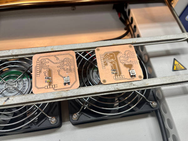
When I zoomed in my board, I saw that underneath the resistor there was a small amount of solder. After doing some measuring it turned out it wasn't a problem, but initially I thought it was a problem so my instructor kindly showed me how to get the component off with hot air gun.
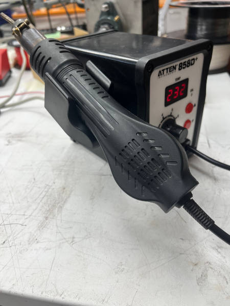
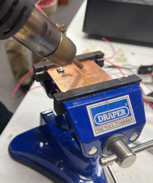
This was in interesting experience. The hot air of course should not be too hot and you should target the soldered spots carefully and away from the other components. It came off quite nicely. Then we took off the extra solder and just put the resistor back. Of course, the hot air gun cannot be used without someone who has a licence to do these kind of works.
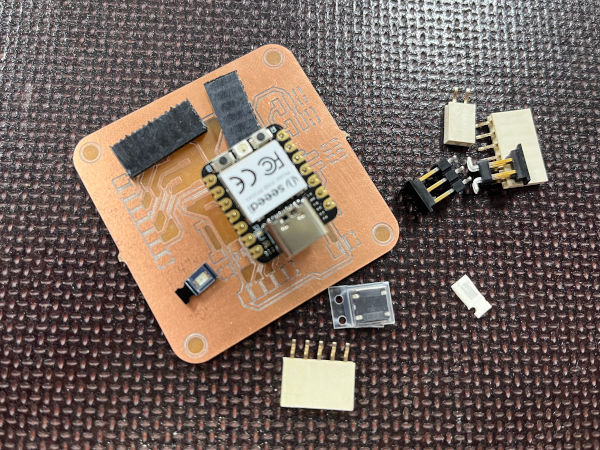
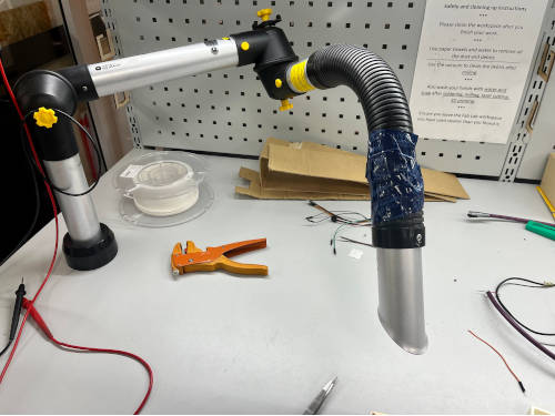
Now I gathered the rest of the components and when on to soldering station. First thing was to set the air conditioning on, meaning the pipe sucking air. Also I pressed on the soldering unit.
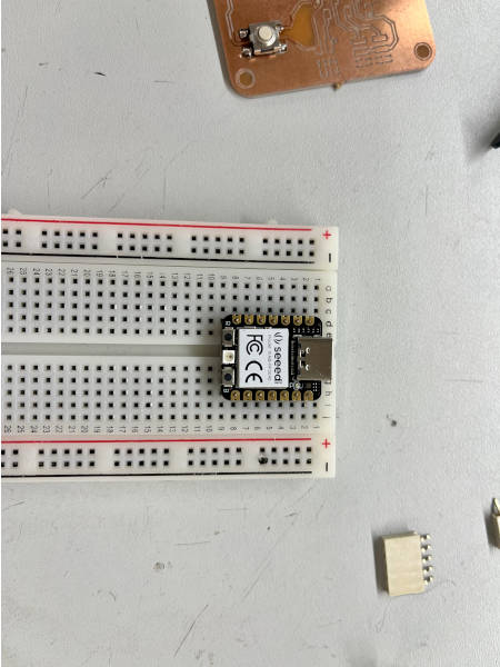
I started with attaching my RP2040 to a breadboard, so that I can solder the pins together in a right angle. Then I warmed up each pin place and added enough of the solder in it. First I managed to do these small round balls what is not good, I was supposed to get the solder to spread better. That requires some practise..
Before attaching the pins and the module to my board, I started with the connective pin headers. For the 8 pin header I used one of 6 and one of 2 and put them together. All in all this was a tiring process. I used tape to try to get the parts staying in the right place. The components are all so small, that they tend to move very easily with big fingers.
After that photo I got into the soldering and forgot to take any more making of -photos! It's a very addictive process. It wasn't easy though, I had to sometimes use the desoldering braid to remove excess solder. Sometimes it also got into places I didn't mean it to. The hardest part might have been the tiny tiny legs that the pin holders (coming to hold the rp2040 pins) had. It felt impossible to heat them up and solder, because the tip of the soldering iron seemed to be bigger then them!
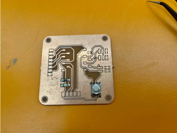
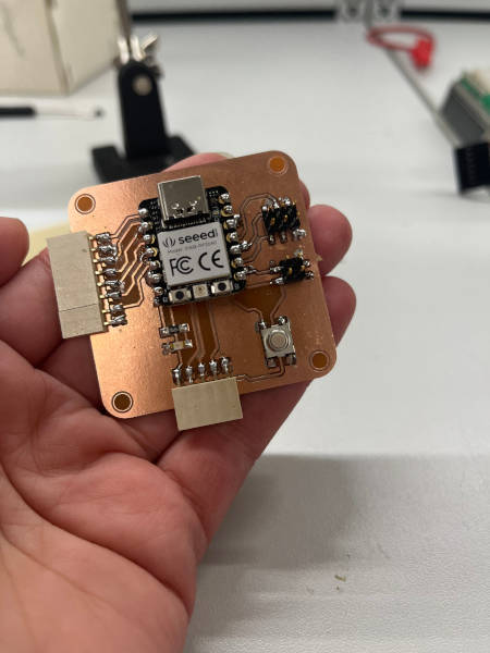
Here is the finished board, with all the component soldered on.
Testing the board
Although my board was ready, I didn't yet know if it was operating. So I plugged in the rp2040 to my computer and opened up Arduino IDE.
To start, I first tried if the RP2040 was still working by blinking the built-in LEDs. It worked fine.
Then I grapped some code from Arduino pages to try to get the external LED blinking. Nothing was happening. I stared at the code but didn't see anything wrong with it. At this point it seemed there might be a problem in my soldering. My instructor helped me with a microscope, and it was seen that I had caused one short-circuit with solder spredding from a pin to ground.
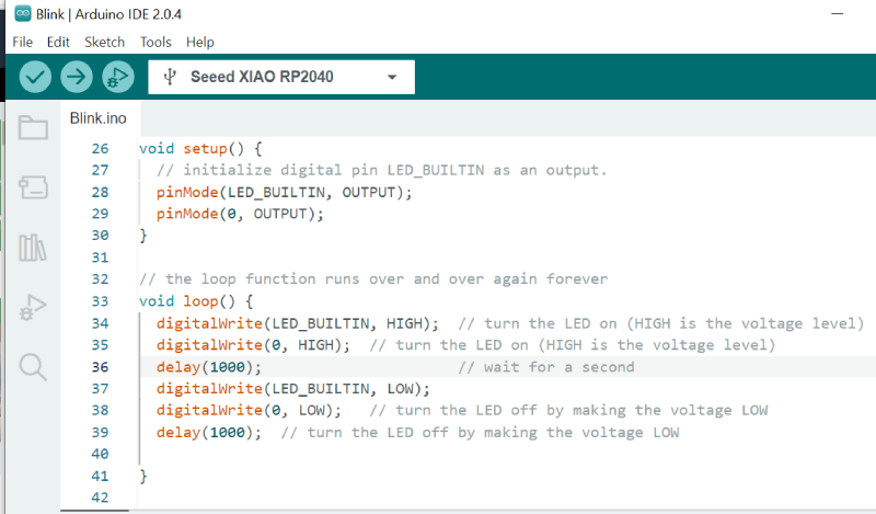
After the excess solder was taken out, I had a new try. To make the code as simple as possible (and therefore minimizing the possibility of failed code), I just added one external LED to the ready made code from Arduino tutorial here. It is the built-in example.
The code made the built-in LED blink. So I added the external LED as an output, and then with DigitalWrite set the LED to turn on and off. The external LED was connected to pin number 0 on RP2040. I ran the code, and it worked! What a feeling.
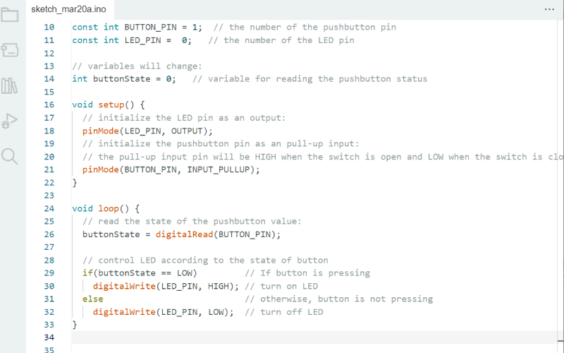
So now I wanted to add the button function in. I again searched for a code from Arduino as they seem to work well and found this.
In the code the button controls the LED going on or off.
So I changed the constants pin numbers to LED=0 and button=1 as they are connected in my board. In PinMode the LED is set to an output and the button as an input. Finally in the code it is set that if the ButtonState is low, turn on LED. If not, turn it off. And it worked well again!